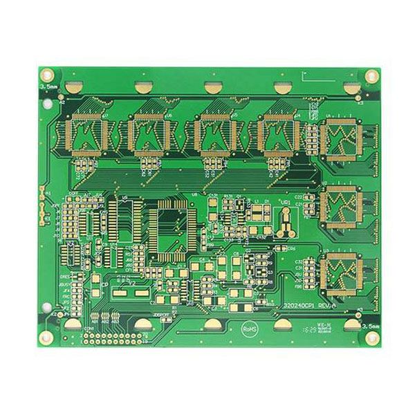
Multilayer PCB

What's the definition of a multilayer PCB?
Unlike a Double-Sided PCB which only has two conductive layers of material, all multilayer PCBs must have at least three layers of conductive material which are buried in the center of the material.
Many printed circuit boards have one or two conductive layers, being built on either a double-sided or a single-sided substrate. A multi-layer PCB is designed and manufactured using several layers of base material. Generally speaking, any board featuring at least three conductive layers is included in this category.
Multilayer PCBs are constructed using a ‘sandwich’ model, featuring numerous double-sided conductive layers separated by a corresponding number of insulating material sheets. These must all be bonded and laminated together under high pressures and temperatures, such that no air gaps remain and the final PCB assembly is sufficiently robust.
How Are Multilayer PCBs Made?
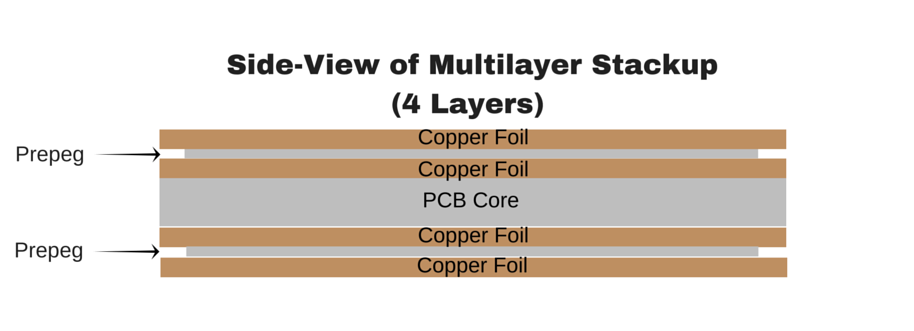
Alternating layers of prepeg and core materials are laminated together under high temperature and pressure to produce Multilayer PCBs. This process ensures that air isn’t trapped between layers, conductors are completely encapsulated by resin, and the adhesive that holds the layers together are properly melted and cured. The range of material combinations is extensive from basic epoxy glass to exotic ceramic or Teflon materials.

The figure above illustrates the stackup of a 4-Layer/ multilayer PCB. Prepeg and core are essentially the same material, but prepeg is not fully cured, making it more malleable than the core.The alternating layers are then placed into a lamination press. Extremely high temperatures and pressures are applied to the stackup, causing the prepeg to “melt” and join the layers together. After cooling off, the end result is a very hard and solid multilayer board.
Benefits of Multilayer PCBs (compared to Single or Double-sided PCBs)
- Higher assembly density
- Smaller size (considerable savings on space)
- Increased flexibility
- Easier incorporation controlled impedance features.
- EMI shielding through careful placement of power and ground layers.
- Reduces the need for interconnection wiring harnesses (reduces overall weight)
Applications of Multilayer PCBs
While the weight and space benefits of multilayer PCBs are especially valuable for Aerospace PCBs, multilayer PCBs are also beneficial to applications where “cross-talk” levels are critical. These are a few other the applications using multilayer printed circuit boards:
- Computers
- File servers
- Data storage
- Signal transmission
- Cell phone transmission
- Cell phone repeaters
- GPS technology
- Industrial controls
- Satellite systems
- Hand held devices
- Test equipment
- X-ray equipment
- Heart monitors
- Cat scan technology
- Atomic accelerators
- Central fire alarm systems
- Fiber optic receptors
- Nuclear detection systems
- Space probe equipment
- Weather analysis